Since the 555 timer is able to operate on frequencies, measured in thousands of Hertz, you can use it to determine the speed of human reactions. You have the opportunity to arrange a competition with friends to check responsiveness, as well as figuring out how the reaction rate depends on your condition, time of day, or how well you slept the night before.
Before proceeding, I should warn you that this scheme has more connections than those schemes that you did earlier. Conceptually it is not much more difficult, but it requires a large number of compounds and can be performed only on a breadboard, which has 63 number of holes. Because we can divide our work in several stages, it will help you to identify errors, if any. You will need:
- 4026 chip. Quantity is 4 units. (actually you need only 3, but buy another in case any output).
- 555 timers. Quantity is 3 PCs.
- Buttons (single-pole switches without fixation). Quantity is 3 PCs.
- Three led digital indicator or indicator to display three digits. Quantity is 1 piece.
- Breadboard, resistors, capacitors and multimeter, as usual.
Step 1. Indicator
You can use three separate LEDs for each digit, but I suggest you buy a semiseg-mentnyj VS56-11EWA led production company Kingbright. It contains three semisegmentnyh digital indicator in one case.
You will need to install it on the right side of your layout boards in its middle, so that the indicator closed its middle. Slide the indicator layout fee as shown on Fig.1. At this stage you must insert any other components.

Figure. 1. After adding a resistor with resistance 1 KOhm between common cathode and the negative power supply output you can use positive voltage for ignition of each segment of the indicator turns
Now install your power supply voltage equal to 9 in, and connect the negative terminal to a number of holes that are located on the right side of the layout of the Board.
Insert a resistor with resistance 1 KOhm between negative power supply output (GND) and each of the three pins: 18, 19 and 26 of the indicator VS56-11EWA, which is a device with "common cathode", which means a shared connection all cathodes of all LEDs (light-emitting diode segment) each digital indicator. (Indicator PIN numbers showing on Figure. 2. If you use another type of indicator, you should see the corresponding reference data sheet to find what conclusion (conclusions) must be connected to the negative conclusion power source (land)).
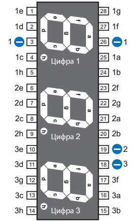
Figure. 2. The seven-segment indicator VS56-11EWA: contains three lights in one housing and can be controlled by three tandem decimal 4026 counters. PIN numbers are shown on the IP. Segments from "a" to "g" indicator digits 1 identical conclusions identified from "1a" to "1 g". Segments from "a" to "g" 2 digits indicator correspond from ' 2A to 2 g. Segments from "a" to "g" indicator 3 digits correspond from the "3A" to "3 g"
Turn on the power source and tap the end wires Bared from the positive power supply output, each row of holes that match the conclusions of all the segments of the indicator. You should see that each segment will light up as shown in the Fig.1 for "c" segment figures 1.
Each decimal digit from 0 to 9 is displayed by a group of specific segments. These segments on the display always denoted by lowercase Latin letters from "a" to "g" (the GeneralFigure 3). Often used additional led to display the decimal point, while we will not use it in figure it is marked with the letter "h".

Figure. 3. The most commonly used and applied digital indicator consists of 7 led segments, each of which has a letter designation, as shown in the figure, plus a segment to display decimal point
Take a look at Fig. 2where-11EWA BC56 indicator shows from the company Kingbright, and next to each withdrawal you'll notice designation of all relevant segments of the indicator. You can check the indicator connecting wire from the positive power supply output to each conclusion segment, to make sure that this segment lights up.
By the way, this indicator has two dual output, numbered digits 3 and 26 with the "-" icon in the small circle located near the numeral 1. This symbol indicates that these two findings are intended for connection of wire from the negative power supply output (GND) the first digit indicator. Why two instead of one? I do not know. You only need to use one, but because it is a passive element, it does not matter if you leave unused findings entered. You need to take care only about how not to accidentally apply positive voltage on them, as this may cause short circuit.
Digital placards has no power source or custom logic. It's just a set of light-emitting diodes. In fact this has not much use until we can determine how to incorporate LEDs, United in a group is and will be our next step.
Step 2. Counter
Fortunately, we have a chip with the designation 4026 which, receiving impulses, believes them to be and issues a corresponding output voltage, which in turn can manage 7-segment indicator so that it will display digits from 0 to 9. The only problem is that this is a legacy type chip CMOS technology (which means Complementary Metal Oxide Semiconductor-complementary metal-oxide semiconductor CMOS), which is sensitive to static electricity. Before proceeding, the following footnote read precautions that should have to perform when working with such chips.
Grounding your body
To avoid trouble, which can happen when you're feeding voltage on the circuit and that nothing happened, you should make sure that you comply with the following precautions when working with legacy generation CMOS technology with chip (CMOS) (which often have designations from 4000 and above, for example, 4002, 4020, etc.).
Chips often come in such a way that their conclusions are shorted pin black sponge. This sponge has good electrical conductivity, and you should keep them in this form until they are needed.
If chips come in a plastic tubular packages, you can remove them and nakolot their findings at pin a piece of conductive sponge or, if you don't have a sponge, use aluminum foil for this purpose. The idea is not to give any one found the chips get much greater potential than other potential output.
When working with components CMOS (CMOS) the grounding is very important the running. I found that in dry weather, static electricity builds up on me when I walk in socks on the floor covered with linoleum, containing a certain amount of synthetic fibers. You can buy a wrist strap to ground your body, or just touch a large metal object such as a metal cabinet for the folders before you handle your PCB. I have trained myself to work in a position where my foot sock touches the metal cabinet that solves this problem.
Never need to solder a chip CMOS (CMOS) when they filed under supply voltage.
Grounding the tip of your soldering irons, too, a good way to protect it from static electricity.
But it's best not to solder a chip CMOS (CMOS) at all. When you are ready to "immortalize" device, move all components with a layout tabs on perforated circuit board, solder to it appropriate for such a chip socket, then insert it into the socket. If you have a problem in the future, you can remove the defective chip and insert properly.
Use a grounded conductive surface on your desktop. The cheapest way to do this is to put a piece of aluminum foil and grounded it (using the "crocodile" with a long wire) by connecting this wire to a radiator, or in a large steel object. I prefer to use a piece of conductive sponge for the surface of my desk. This is the same type of sponge, which is used in the packaging of integrated circuits. However, this sponge is quite expensive.
Switch off power supply and connect the wires from the power supply to the top of the layout of the motherboard as it is necessary for this experiment, we in this case would require a positive and a negative voltage on the two edges of the layout of the Board. Wiring of power supply, you can look at Figure. 4. If Breadboard has no colored columns marking the holes intended for power connection, I suggest that we use to designate them colored markers (Sharpie Sharpie is a popular brand of markers/markers in the United States, including indelible and an indelible composition) to avoid errors when connecting supply with reverse polarity, which can lead to failure of components.

Figure. 4. When assembling the circuits near the chips on both sides of your layout boards are very handy to have tires supplying voltages with contacts, to which are connected the wires from the power source. For a diagram of the timer to measure human reaction need to supply voltage 9 in such capacity condenser with 100 µF, which must be installed as shown in the figure. If the left and right side of your layout boards do not have colour marking columns pin holes (Shin), I suggest you do so using the markings of indelible color markers
When powered microchips 4026 counter from the source with voltage 9 to it had sufficient power output to enable our indicator LEDs. You should make sure that chip focus correctly, and then paste it in the Layout tab next and slightly above your three-digit indicator, leaving only one empty between them a series of pin holes.
(DiagramFigure. 5connecting chips findings depicted) 4026 to the indicator. Arrow keys with numbers show the indicator PIN numbers, to which must be connected to counter these findings.

Figure. 5. Chip is the decimal 1S3 4026 counter and is three-digit 1S4 digital 7-segment led. Arrows with figures showing the indicator PIN numbers, to which must be connected to the corresponding output counter
On Figure 6 shows the location and purpose of each chip output 4026. You should compare it with the schema contained in the Figure. 5.

Figure. 6. Decimal counter 4026 is performed on the chip CMOS (CMOS), which receives the clock clock signals to output 1, believes them to be from 0 to 9, the code in the deshifruja output signals corresponding to interface 3-digit seven-segment digital indicator
Should be added to the schema button between the positive pole of the power supply and output 1 4026 counter and also connect this output through resistor with resistance 10 kΩ power supply to the negative pole (Earth) to maintain negative capacity at this conclusion until a button is pressed. You should make sure that all connections to the power source are correct, and then apply the supply voltage. You should find that when you will press the button slightly, the counter will count and display the digits from "0" to "9", then start with "0". You may also find that sometimes the counter chip incorrectly perceives the button and immediately starts counting two or more units in one-touch. I will return to this issue later.
Segments of the LEDs will not shine very brightly, as consistently connected resistors R4-R6 with resistance 1 kΩ will leave them exactly as much power as they need. These resistors are necessary to limit excess current, coming from the counter.
|
Basic information |
| Counters and segment indicatorsMost enumerators receive the stream of pulses and predeljajut their group findings in a specific follower. Decimal 4026 counter is unusual in the sense that he's on their weekend conclusions issues such Combi nation of voltages that are specially designed to put glow segment indicators.
Individual counters on their outputs create positive Nye signals (they are "sources"), while others create negative signal on the output (they are "receivers"). Some control but RAM to display requires positive input the signal sig. Such indicators are called indicators with common cathode. Other indicators required negative input signals and Nye because they are called indicators with common ELN House. 4026 counter positive output signals, so it needs an indicator with a common cathode. Double-check reference data sheets for each chip counter, to determine what kind of power they consume and what power they can produce. CMOS chip (CMOS) are somewhat obsolete, but they are very useful for those who have chosen electronics as a hobby, because they can use a wide range of supply voltage in the case of integrated micro circuits 4026 counter This range extends from 5 to 15 in Other types of chips fell. in this sense, is not as versatile. Most enumerators can be sources or when emnikami only a few milliamps output power. When chip 4026 running from the power supply 9 v, it can be a power source with a value of approximately up to 4 Ma for each output. This is quite enough for operation tion led seven-segment indicator. You can include resistors at each successively outputting a counter and on each input digital indicator, but Bo was more simple and less expensive solution, this time the use of a single serial resistors for each indicator the numbers between the overall conclusion of the cathodes and LEDs. In the experiment, which I describe is such a decision. The disadvantage is that the figures that require the use of only two SEG cops in the indicator (for example, the digit "1") will glow brighter than those that use a lot of segments (for example, the digit "8"). If you want your trehrazrjadnaja display from the professional point of view looked bright and flawless, then you need to use transistors to control the conclusions of each segment in each digital display. Alternatively, the chip can be used that to strengthen current contain many operational amplifiers. When decimal counter when the score reaches "9" and switched to a value of "0", it generates momentum with its output "signal transfer. Using this output, you can run another counter which already would perform by tens. Output signal transfer this second counter can be connected to the third, which would counter by hundreds, etc. In addition to the decimal hexadecimal there are counters counters (who believe up to 16), octal (up to 8), etc. Why would you need anything not counting in tens? Imagine that you have a digital clock with four indication that perform account differently. Extreme right digit changes its values after reaching a "10". The next digit to the left of the view to "6". The first digit units hours, which felt to "10", produces a signal transfer scheme, which deems to "2", and gives the next signal transfer. The leftmost digit can be either disabled or showing "1", when you display the time in 12-hour format. Naturally, there are counters that are specifically designed to perform this work. Counters have a number of Governors of conclusions such as: "the clock" (Disable clock), which indicates to ignore his counter input pulses and suspend, or "freeze" indication; "allow output indication" (Enable display), which allows signals to the outputs chip for their subsequent indication; finding the reset button (Reset) that resets the result counts. 4026 counter needed a positive signal at the input to make active every managing withdrawal. When findings grounded, their functions are disabled. To perform a countdown counter 4026 and display the result on the scoreboard, you must ground the conclusions "clocking" and "Reset" (to disable their functionality) and attach the positive potential to conclude "allow an indication (to activate the output). Pay your attention to the Fig. 6where shows pin assignments. |
Assume that you have successfully collected schema with one control counter digits seven-segment indicator, and now want to add another two counters, which will manage the two remaining bits of indicator. The first counter is designed to count units, the second dozen, and the third hundred.
On Figure. 7 I will continue to represent the schema using the arrows with the figures, which will show you what counters should be connected to the relevant conclusions of the three digital indicator. Otherwise, the scheme will represent a tangle of wires, intersecting with each other.

Figure. 7. This test scheme is designed in such a way as you probably would like her place on the breadboard, that will allow you to manage the counter manually to verify that the scoreboard changes testimony sequentially from 000000 to 999. The value of the schema components: R1-R6-resistors with resistance equal to 1 KOhm; S1, S2, S3-banana one-positional button without fixing, normally open; IS1, IS2, IS3 — decimal 4026 counter chip; IS4 is a three-digit digital led display with common cathode 7 segment; C1-capacitor electrolytic, smoothing with a capacity of at least 100 µF. Connect wires IS1, IS2 counters findings and conclusions with IS3 IS4 indicator whose numbers are indicated next to the arrows. In order not to clutter the diagram, the real wired connections were not shown. Check the connections according to diagram pinout indicator (see fig. 2)
In this place you can embrace the horror of such a number of compounds, but in fact, when you use a layout Board, this should not take more than half an hour to complete this part of the project.
I suggest that you try to do it because there's something magical when the display device performs account from 000000 to 999 "all in itself, and I chose this device, because it also has a lot of value from an educational perspective.
S1 button connects to the conclusion "clocking" (Disable clock) chip IC1, so that when you hold the button pressed, the meter will not be considered. Because chip IC1 manages the following counter IC2, and he, in turn, controls the third counter IC3, if you pause the counter IC1, the other two the same chips will wait for an invoice. Therefore, in this scheme, you will no longer need to use the findings of the "clocking" (Disable clock).
Button S2 is connected to the reset button (Reset) all three counters, so when you hold it down, they all need to be reset.
S3 button sends positive pulses output manually "Clock" input of the first counter.
In parallel, all the buttons S1, S2 and S3 are connected resistors with resistance 1 KOhm, but connected to the negative power supply output ("Earth"). The idea is that when the button is pressed, these resistors firming will support potential conclusions close to earth potential (zero). When you click one of the buttons directly to the positive supply voltage implemented chip that could easily override a negative voltage. Thus, the conclusions remain either explicitly positive or in explicitly negative position. If you disconnect one of these podtjagivajushhih, then you will probably notice an unstable state of digits on the display. (The digital indicator has several from unattached conclusions, but they do not create any problems, since the indicator is a passive element that simply carries out the inclusion of led segments).
Footnote
You should always connect the findings of CMOS (CMOS) chip so that they were either positive or negative.
I assume that you are already hooked up all the wires according to the previous diagram. Then using small pieces of single-conductor wire 22 AWG (0.64 mm) you'll need to make all the connections of the conclusions of the panelek chipset ICI, IC2 and IC3 IC4 indicator but with a digital (see. Figure. 7).
Switch on the supply voltage and then click S2. On your display you should see 3 scratch.
Each time after pressing the S3 account result will increase by 1. If you again press the button S2, the counters and the indicator will take the original zero position. If you hold down the button S1, while periodically pressing the S3 button, the counter will remain in certain fixed ("frozen"), ignoring all counting impulses from the button S3.
No floating conclusions!
Chip KM0P-(CM0S-) strukturyjavljaetsja on its "nature" hypersensitive. Any output that is not connected to a power source or earth, referred to as floating. Such findings may be an antenna that will respond to the slightest environmental changes chip Wednesday.
4026 counter chip output, which is labeled as "clocking" (Disable clock). Technical data manufacturer helpfully inform us that, if you do this output positive voltage, the integrated circuit will stop by and "numbs" indications on the display. If you don't want that, then you can just ignore this conclusion, and leave it disconnected until at least perform the test chip. This is actually a very bad idea!
Unfortunately, the reference data does not provide information about the that for the proper functioning of the heartbeat function clocking prohibition should be disabled by connecting the output of "clocking" (Disable clock) chip to a negative conclusion on the power source ("Earth"). If you leave this conclusion "floating" (and I'm telling you this from my experience), the chip will work with errors and useless.
All input conclusions must be either positive or negative, unless otherwise indicated.
|
Basic information |
| Bouncing when switchingWhen you click Switch B3, I suppose you found confirmed that sometimes the testimony of placards is increased by more than 1. This does not mean that something was done wrong when installing your card or your components; you just to bljudaete effect, which is called bouncing.
If we consider this effect at the microscopic level, not the contacts inside the switch button not prima cabins each other smoothly, securely and instantly. They calm down, before hesitating a few microseconds; and mikroshe Ma for the counter registers these fluctuations in a series featuring pulse, and does not perceive as a pulse. To eliminate flickering, you can use different schemes. The easiest way is with the application of a small capacitor that connects in parallel switch to suppress these changes signal; but this solution is far from perfect. I will return to the topic eliminate bounce later. Bouncing buttons B3 is not a problem for this scheme because we then this button going to replace the 555 timer which will GE nerirovat clear impulses without any "bounce". |
Pulse generation
555 timer chip is ideal to control the chip count. We've already covered how to use the 555 timer, you can generate a sequence of pulses that make the speaker buzz. On Figure. 8 I cite the same schema (but in a more simplified form) power source connection in this project. I am also showing connection 2 and 6 conclusions as it is most commonly performed using wires that goes above the hull.

Figure. 8. Basic scheme works in avtokolebatelnom mode, which gives you the ability to control the decimal counter collected on the earlier diagram. Output frequency should be equal to approximately 4 Hz (pulse per second). R7 is a resistor with resistance 1 KOhm; The R8 is a resistor with resistance 2.2 kohm; C2-Electrolytic Capacitor with a capacity of 68 µF; C3 — 0.1 µF capacitor; Ic5-555 timer chip
For this experiment, I propose that the initial values of the components have been chosen so that the generation of pulses with a frequency of 4 Hz only. Any large frequency generation does not give you the opportunity to test the correctness of the execution account.
On your layout fee just above IC 555 timer chip set IC1 IC5 and associated components that must be connected to it. You should not leave any gap between the circuits. Disconnect the resistor R3 and S3 button and connect the wire directly between the output 3 output 1 IC5 chip chip generating positive pulse at its output (output 3). When the capacitor has reached the charge, equal to 2/3 supply voltage, the 555 timer at that time indicated that the need to complete the formation of a positive momentum and switch the output back to its original state with voltage the relevant negative conclusion power source ("Earth").

Figure. 9. the withdrawal mode bistable 6 555 timer constantly voltage equal to a negative conclusion on the power source ("Earth"), therefore, a positive signal at the output of the timer does not stop until you prinudite it do so by negative impetus to conclusion 4 (reset)
Good, but if in this case there is no capacitor, then there is nothing that could return the timer to its original state. Then the output will be to continue formation of positive momentum. Nevertheless, output 4 (reset) retains the highest priority for timer switch. After reset signal output the timer will remain negative, that always happens, until once again you do not switch timer, reducing the voltage at pin 2, i.e. issuing a start signal. This causes the timer to switch back, and he again will generate a positive voltage on the output.
Next, let's consider the conclusions for the 555 timer bistable mode (with two stable States).
- Feed the negative momentum for withdrawal of 2 leads to the beginning of a positive signal at the output of the timer.
- Feed the negative momentum on the 4 output returns the output signal reset timer with a voltage corresponding to a negative conclusion on the power source ("Earth").
- The timer is always in one of these States. During their stay in these conditions can last indefinitely.
While normally leave conclusions 5 and 7 timer turned off because we translate them into extreme States that feed any arbitrary signal on these conclusions will be ignored.
In the bistable mode 555 Timer turns into one big trigger. To avoid any uncertainty, we are using podtjagivajushhih resistors on the findings of a 2 and 4 chips support the positive voltage, but negative impulses on these findings may prevail when we want to enter 555 timer the opposite State. 555 timer circuit that operates in bistable mode and managed two buttons, refer to the Figure. 10. You can add this schema to previously collected. Since we are going to connect the output chips IC6 555 timer (3) found 2 (prohibition of clock) chip IC1 topmost counter schema, you can disable the button S1 and R1 from this finding, as it was in the previous diagram (see. Figure. 7).
Now again turn on the supply voltage. You should find that the scheme runs through exactly the same as before, but when you push a button S4 stop counters ("frozen"). This is due to the fact that chip IC6 555 timer that operates in bistable mode, sends a positive signal with its release on output 2 (prohibition of clocking) counter IC1. Counter will continue to receive a stream of pulses from chip IC5 (555 timer operating in avtokolebatelnom mode) (see. Figure. 8), but until the withdrawal of 2 positive potential remains counter, the counter will simply ignore these impulses.
Now click the S5 (see. Figure. 10), which switches the timer 555 (chip IC6), which now appears negative signal. This will lead to a resumption of the account.

Figure. 10. Add 555 timer bistable mode to determine the reaction of the human tester would lead to stopping the countdown after touching a button and store the result. R9, R10:1 k; IC6:555 Timer
We came very close to finalizing the scheme. We are now able to reset the counter (the button S2), run by (S5 button) and wait until the user stops the account (button S4). The only thing we missed this way to unexpected signal for subsequent stop scheme.
Latency

Figure. 11. Complete the management part of the circuit: R7, R9, R10, R12, R13 — resistors with resistance 1 KOhm; The R8 is a resistor with resistance 2.2 kohm; R11 is a resistor with resistance 330 kohm; C1-capacity Electrolytic Capacitor 100 µF; C2-Electrolytic Capacitor with a capacity of 68 µF; C3, C4, C6-0.1 µF capacitor; C5-capacity Electrolytic Capacitor 10 µF; S1, S2, S3-banana const button without detent; Ic5, IC6, IC7-555 timers
Let's install another 555 timer which will work in monostabilnom mode. Run it with 2 output using negative pulse, and the timer will emit a positive signal that will last, let's say, 4 sec. At the end of this time his output returns to its original state when it will be a negative signal. We can connect this output (output 3 chip 1S7) concluded 4 chip 1S6 and use differential pulse from a positive to a negative condition (pulse slice). This difference can be applied instead of S5, which we previously pressed for commencement.
Collect and check the new scheme, which is shown in Fig. 11 and added another 555 timer chip 1S7 is located just above the chip 1S6. When the signal at the output of microchips 1S7 will switch from positive to negative status, it's doing on conclusion 4 (reset) chip 1S6, will toggle its output in the original negative status, which allows you to start the counter account. Thus, IC7 chip takes the place of the Start button S5 account. So now you can unsubscribe button S5, but retain the pull-up resistor R10, because output 4 (reset) chips IC6 should remain positive, the rest of the time.
Such a system would work, since I used the capacitor C4 to connect output chip IC7 found dumping chips IC6 (4). This capacitor only allows short-time pulse differential from positive to negative voltage level (ground level), and the reverse delta chip output has no effect on chip IC6.
Final scheme on Fig. 11contains three 555 timer connected together — they are located above the topmost junior counter, t. e. chip IC1. To signal to the user I also added. On Fig. 12 see a picture of my running this layout scheme.
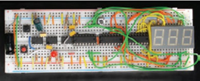
Figure. 12. Complete the timer scheme to determine the response of a man barely fits on a breadboard, which contains a number of 63 holes
Because the schema is complex enough, let some total, resulting in a sequence of events that occurs during its work. In the following steps need to be guided by the scheme which provides for the Fig. 11:
- The user clicks a button S4 to launch delays, resulting in switching chip IC7.
- For a few seconds until the charging capacitor C5, IC7 chip output remains in a State of high level corresponding to the positive power source.
- Then exit chip IC7 becomes low, equal ground potential.
- This difference of IC7 chip issues through the capacitor C4 on integrated circuit 4 output IC6.
- The output of the chips IC6 switches to a low level and is registered in this State.
- A low signal output level chips IC6 lights signal led.
- The same low level output signal chips IC6 served also on the counter chip 2 output IC1.
- Low level voltage on this output IC1 chip provides an opportunity to counter IC1 start account.
- The user noticing the illuminated signal led, presses the stop button S3.
- S3 button attaches 2 IC6 chip output to ground.
- The output of the chips IC6 switches to high-level State and remains in this State.
- High-level output chips IC6 disables signal led.
- High-level output 3 output chips IC6 also served on output 2 (prohibition of clock) chip IC1.
- High level output voltage chip counter 2 IC1 stops by, which he has.
- After studying the result on the display, the user clicks the button S2.
- This button S2 delivers positive voltage on all findings of 15 chips IC1, IC2, IC3.
- Positive voltage resets the counter.
- The user can now try again.
- In the meantime, IC5 chip runs continuously.
If you understand the work on the flowchart, I introduced Figure. 13.

Figure. 13. the operation of the device to determine the response of the person, which is given in the form of flowcharts
Use of the device to determine the response of a person
From this point on, you can check the schema. When you first turn it on, it starts by, which is somewhat annoying, but that's easy to stop. To do this, click S3. Press S2 to reset the readings.
Now click the S4. After that, nothing seems to happen-this is the basic idea. Delay loop starts in stealth mode. After a few seconds, the cycle ends and the led signal lights. At the same time begins. To stop him, the user as fast as possible should press button S3. "Freeze", showing how much time has elapsed.
Now there is only one problem-the system is not yet on-calibrated. She still works in slow motion. To make the frequency of generating equal 1000 Hz rather than 3 or 4 Hz, you need to change the resistance of the resistor and capacitor container vremjazadajushhego, IC5 chip are connected to.
Replace resistor R8 "potentiometer 10 kΩ resistance and capacitor C2 condenser capacity 1 µF. If the potentiometer set to maximum resistance, this combination of components will lead to the generation of pulses with a frequency of 690 Hz. When did you begin to decrease the resistance of the potentiometer, approximately half of the way timer will generate at a frequency of 1000 Hz.
And how exactly to define this position potentiometer and accordingly this frequency? The ideal solution would be to connect the oscilloscope to the exit IC5 chips. But it is more likely that you don't have an oscilloscope, so I suggest a couple of other ways.
First as a capacitor C2 condenser instead of par value 1 μf, select capacitor 10 µF. Because you have increased capacity in 10 times, then you are in 10 times reduced frequency. The leftmost digit on your scoreboard should now perform the countdown in seconds and reaching number 9, switch to 0 and perform it every 10 seconds. You should just adjust the potentiometer ", checking account while using the stopwatch. When you make sure the setting is executed exactly, again it is necessary to replace the capacitor C2 with a capacity of 10 µF at capacitor 1 µF.
In this case, only one issue remains the accuracy capacitance can vary between 10%. If you want to fine-tune your human response identifier, you can proceed as follows.
Unplug the line cord connected to the conclusion of the older chips 5 counter IC3, and replace it with fresh todiodom with serially attached resistor with resistance 1 kΩ, which must be connected to the negative pole of the power supply (ground). 5 output is the output of the output signal transfer (carry), which represents a positive impetus, when the counter IC3 doschityvaet in a forward direction until the "9" and switches back to "0". Because counter IC3 must take tenths of seconds, then you need to transfer signal at pin 5 appearing every second.
Now run the scheme so that it worked for a minute, and using your stopwatch, count the number of blinks of the led. So you can adjust the frequency with an accuracy of ± 1 Hz. If you have a video camera, which is timed display in the viewfinder, then you can use it to check the blinking LEDs.
If the led is blinking too frequently, then it is easy to notice, you can attach a wire from output 5 to another timer 555, who works in monostabilnom mode to create the output, which runs for about a generation 1/10 sec. In this case, you can use the output of the timer to turn on the led.
Further improvements
Needless to say, that every time you finish a project, you can see that there are opportunities to improve it. Here are some ideas in that direction.
- When supply voltage is switched on, it is desirable not to implement the Bill. So it would be great if when you power scheme issued signal its readiness and not perform account immediately. To achieve this you will need to submit a negative impact on output 2 chips IC6 and can be a positive impetus to the conclusion of the 15 (reset) the counter chip. It is possible that this will require another timer 555. I want to give you the opportunity to experiment in this direction.
- Audible signal after pressing "start". Currently, there is no evidence that the "start" button launches a process. To solve this problem you will have to purchase a piezo sounder and connect it between the right side of the "start" button and the plus supply.
- Desirable random delay time interval before the counter will run through. Make electronic components have worked with arbitrary values of time delays, a very difficult task, but one way to accomplish this is to create the schema in which the user completes his finger a couple of metal contacts. The resistance of the skin of the finger will replace resistor of R11. And because the resistance of the thumb each time will be different, that will change and time delay. You also need to perform the adjustment of capacitance C5.
To summarize
So, this project showed how you can manage the chip counter as you can between them connect chip counters, and also showed three different 555 timer functions. In addition, he showed how integrated circuits can communicate with each other. The draft also contains some introduction to calibration scheme after its installation.
Naturally, if you want to get some practical benefit from the scheme, it must fulfil its installation with reliable buttons, especially should be strong button that will stop by. You can easily notice that when people check their reactions, they tend to press on the button hard enough.
Because it was quite a challenging project, then I will continue with more simple and quickly sold devices that will continue your dive into the exciting world of integrated circuits other purposes, namely world of logic chips.