

To increase the capacity of flash chips, made with traditional planar method, it is necessary to increase the density of cells. It is necessary to improve technological process of manufacture. This method itself is very expensive, as well as associated with certain physical limitations. In the case of flash memory the size of the cell is not the best way affects the number of write cycles. Generally, the thinner process technology manufacturing, the smaller the resource cells.
Micron and Intel propose to use for the flash chips layered layout of the 3D NAND. This method of packaging cells immediately brings several advantages. First of all, can significantly increase the capacity of memory chips. Presented chips have at least three times higher density than conventional flash chips. Already at the start of the chip with a mesh-type MLC have the capacity of 256 GB, and version cells TLC – 384 GB.
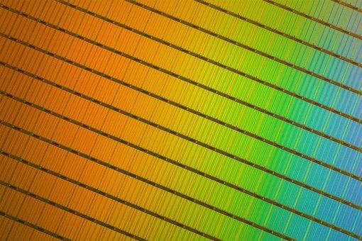
To obtain such results, developers use a 32-layer design combined with the technology of the floating gate. Such internal "storeys" does not affect the physical dimensions of the chip.
Using chips with 3D NAND first generation, manufacturers will be able to increase the amount of disks in the format M. 2 to 3.5 TB. Meanwhile the standard chassis form factor 2.5” will be to offer a SSD with capacity of over 10 TB. Of course, flash 3D NAND chips can be used for mobile devices of various form factors.
The 3D layout makes it possible to increase the distance between cells. In this case, is good news. For making chips in this case you can use the workflow 40-50 nanometers. The increase in the distance between cells allows to increase the reliability. Under these rules production, the number of write cycles should be increased to about 10000. For consumer platforms are more than enough available even 1500-2000 cycles, but for server solutions is a critical parameter. Manufacturers expect when using 3D NAND for enterprise-class SSDS can use the chips in the TLC structure.
It is obvious that the cost of production of 3D NAND chips is slightly higher than standard flash chips, however, given the increasing areal density, the multilevel circuits can provide the best ratio price/volume.
Micron and Intel are going quite quickly bring the technology to market. The developers already gave some partner trial samples of 3D NAND chips with cells of the MLC. Chips with TLC will be available later in late spring. If to speak about mass production, it is the third or fourth quarter of this year. Perhaps in 2015 we will see in the sale of SSD with 3D NAND.